ABOUT
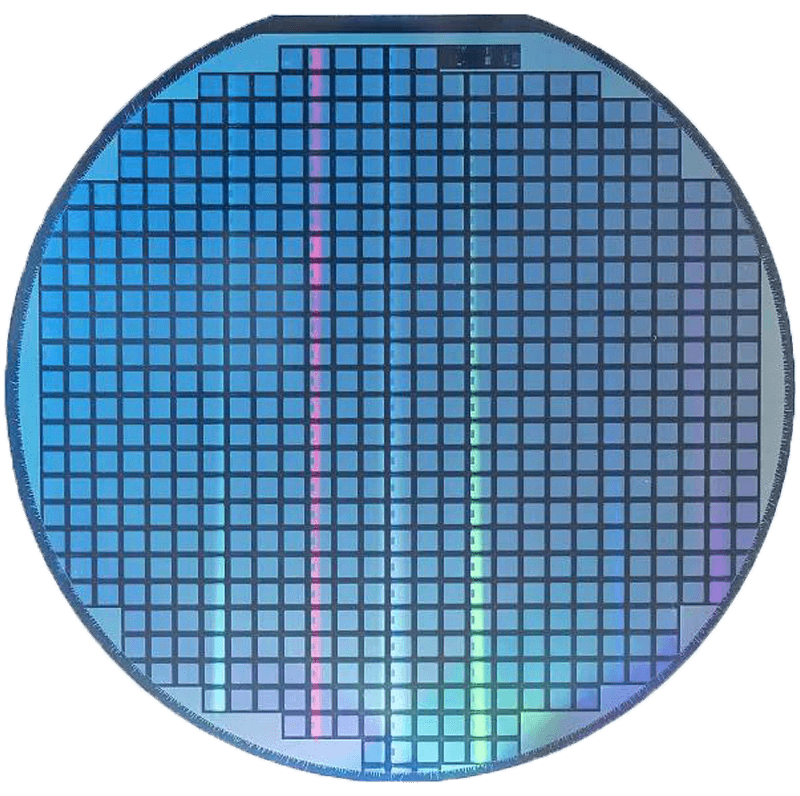
SEMICONDUCTOR WAFERS
Compound semiconductors, as substrate materials for electronic/electronic chips, are 2nd and 3rd generation semiconductor materials, normally refer to GaSe, Ge, GaN or SiC substrates. Compared with traditional silicon substrates, they provide special physical and chemical properties such as large bandgap, high carrier mobility, radiation resistance, and optical transparency.
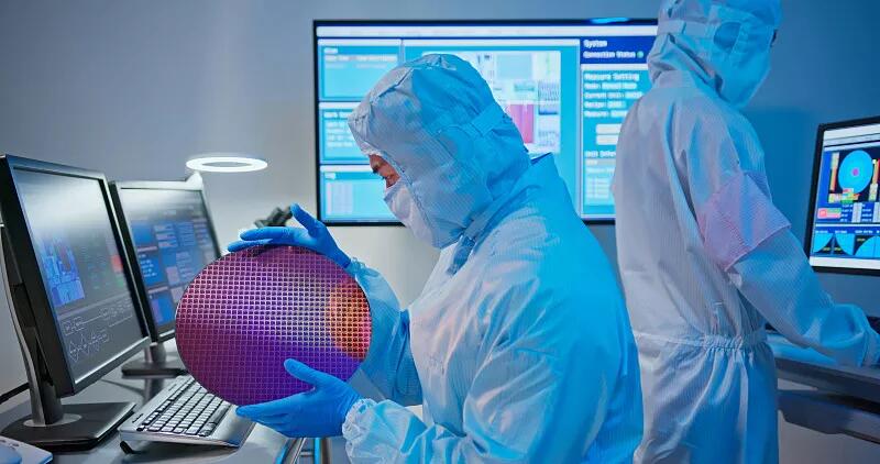
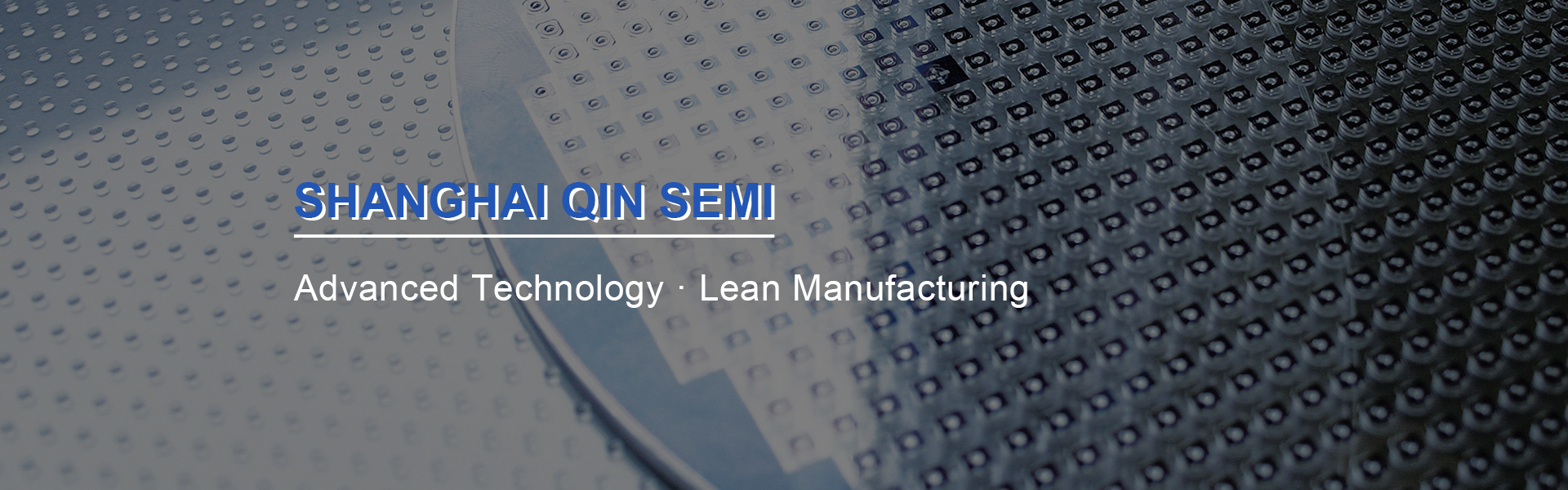
Shanghai QinSEMI Technology Ltd. located in Pudong, Shanghai, was founded in 2020. We are mainly engaged in research and development, production, sales and technical service of semiconductor new nanomaterials in the semiconductor industry. Products and services cover the early chain of compound semiconductor industry, ranging from raw materials, substrate wafers, consuming materials for wafer manufacture, e.g. polishing (CMP) slurry, etch and cleaning solution.